Every hackable connector on ASUS Eee PC 901
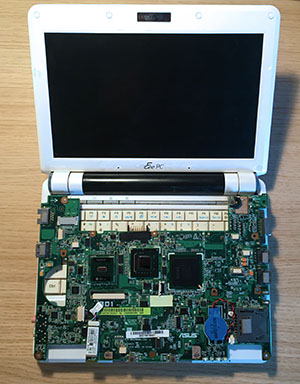
Recently I found my old Eee PC 901 at the bottom of a drawer sitting and collecting dust. It served me well a decade ago and I still have fond memories of it, but by modern standard it’s really obsolete as a laptop. With Intel Atom N270 and 2GB DDR2 RAM at its heart, I’m not sure it’ll win over even Raspberry Pi 4. Yet it is in a good working condition, and I couldn’t bring myself to discard it into the trash bin.
At a peak of its popularity Eee PC family was very popular in the hacking/modding community, so I went on to see if there’s something cool I can do with it. I’ve never really messed with hardware before, so even if it doesn’t work out, I’ll learn something useful from it.
In this post I’ll document interfaces that exist on Eee PC 901 motherboard and present interest for modding. Kudos to the Eee PC community who reverse engineered all of this, I’ll try to cite original sources to the best of my ability, but internet archeology is hard, so apologies if I misidentify any.
Ultimately, the most useful sources were the ASUS original motherboard schematics and component layout, which you can find with a little bit of googling. I also relied heavily on postinga at eeeuser.com (down and gone, but mostly available through web archive), eee-pc.ru (which is also frequently down) and jkkmobile.com. Some specifics about supported protocol versions were found in Intel Atom N270 datasheet and Intel ICH7-M datasheet (south bridge). I also found helpful notes at ivc.no 1, 2, although they focus on Eee PC 701.
Use this information at your own risk! I did my best to cross-check the information between sources, but I haven't tried any of this myself yet!
Summary
- IDE (PATA) master + slave, up to 100 MB/s via
IDE1,IDE2connectors (ASUS proprietaryFLASH_CON) andIDE3(ZIF-40). - 2x SATA 2.0, up to 300 MB/s each via
IDE1andIDE2connectors (FLASH_CON). - 2x PCI-E 1x 1.0a, up to 250 MB/s each via
3GCARDandMINICARDconnectors (mini PCI-E). - 8x USB 2.0, up to 60 MB/s. 3 external USB Type A, 2 internal via
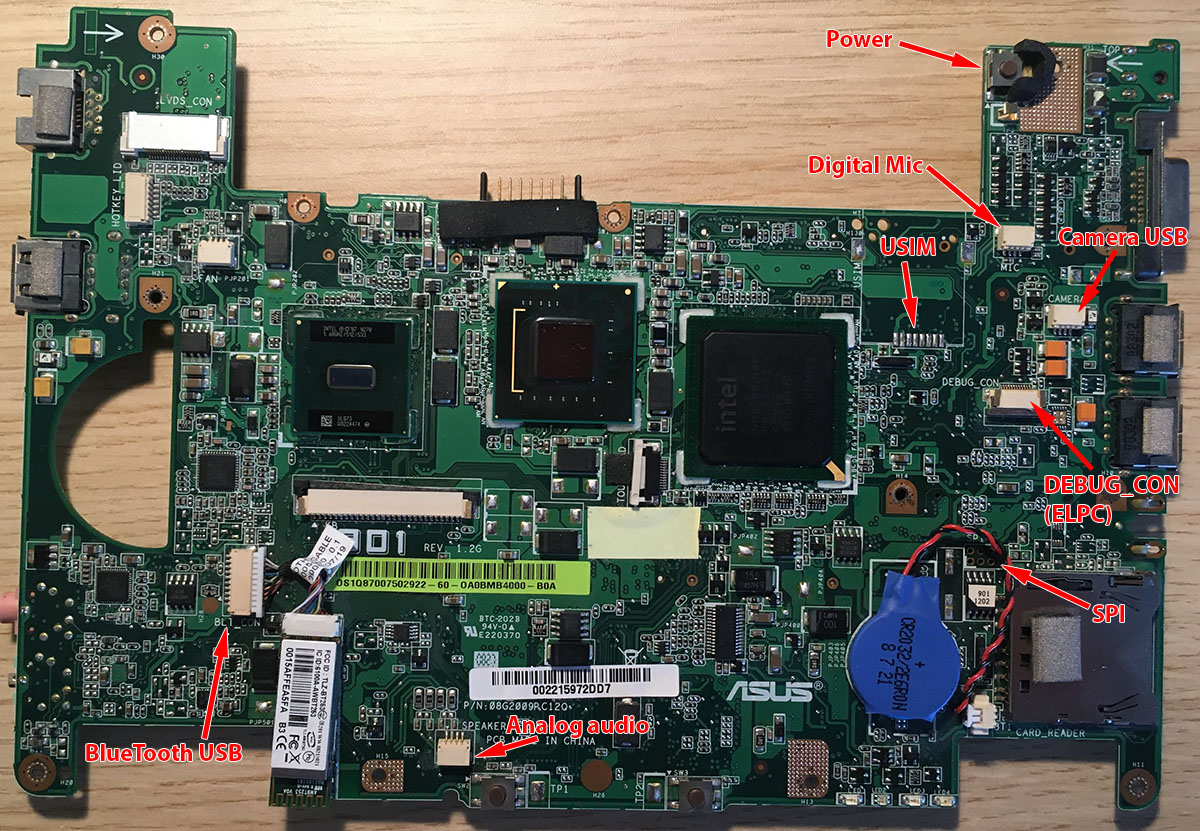
IDE2and3GCARD, 2 internal motherboard connectors (BLT_CONandCAMERA). - Other stuff like internal audio, SPI, ELPC (
DEBUG_CON).
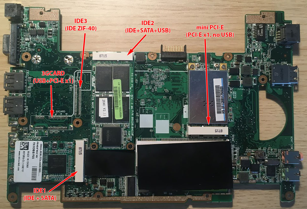
IDE1 and IDE2 (FLASH_CON)
TL;DR: ASUS crammed all possible mass storage buses into a single proprietary interface. It is incompatible with either mini PCI-E spec or mSATA, despite sharing the mechanical socket.
In Eee PC 901 they are used to connect the 50mm, 4 GB internal SSD (IDE1) and the more easily accessible 70mm, 16 GB secondary SSD (IDE2). The same interface was used for internal storage in most other models.
These two are the most notorious in the hacking community for the amount of confusion and wasted money they are responsible for 😅 Mechanically they are identical to mini PCI-E and mSATA interfaces, but aren’t really compatible with either. They are loosely inspired by mini PCI-E, but ASUS engineers liberally rewired them to their own needs.
The complete pinout was published by eeeuser.com member CyberKareca.
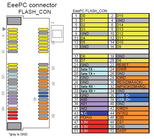
- Yellow, orange and light violet pads are parts of IDE/PATA bus, which is shared between all IDE1-3 connectors (more on it later). tie2 (eeeuser.com) published instructions connecting CompactFlash to it (pdf) using the IDE bus.
- The blue
USB_D±pads are indeed the USB bus, which is about the only thing compatible with mini PCI-E standard, apart fromGND. Sadly only IDE2 connector has them functional on the 901 model. - Most notable are the light-blue pads, which carry a proper SATA data bus signals. Unlike the IDE bus IDE1 and 2 have independent SATA buses, which appear to be usable at the same time and independently from IDE. Eee-pc.ru wiki has a nice instruction on connecting 2.5" SATA disks to it.
So FLASH_CON is more like “the ultimate mass storage interface” than mini
PCI-E. Unfortunately, they are most often referred to as ASUS mini PCI-E,
causing incredible confusion for people looking to upgrade EEE PC’s slow SSDs,
but this is easily a whole separate post…
This port is not electrically compatible with mSATA SSDs, even though the physical connector is the same. According to the internet, it is possible to mod an mSATA SSD to work with this connector, but make sure you are willing to take the risk that comes with a hardware mod (namely, killing your SSD and/or the motherboard).
IDE3
TL;DR: A standard, slow and boring ZIF-40 PATA port on the same bus as IDE1 and 2.
This is FLASH_CON’s little brother which only includes IDE/PATA bus organized
as a
ZIF-40 connector.
The connector was soldered-on in 901’s earlier batches, but in later revisions
was left as bare soldering pads. This connector format was popular with compact
1.8" drives prior to SATA, and there are still some offerings available. Pin
arrangement is basically the same as the
40-pin PATA ribbon cable.
jkkmobile published a guide for connecting an hdd or CompactFlash to this slot, although these days it’s far more practical to use SATA-based solutions.
Because IDE1, IDE2 and IDE3 ports all use the same physical bus, only two can
actually have a device connected at the same time via PATA protocol. However,
as far as I can tell it should be possible to have two SATA devices connected to
IDE 1 and 2, and a PATA drive to IDE 3. Practicality of this approach is
questionable, however, side 1.8" PATA ZIF drives are slow and hard to come by.
Using FLASH_CON to mSATA adapters is a much easier way to get a fast and
high-capacity storage without any soldering.
3GCARD
TL;DR: A regular mini PCI-E slot, requires soldering to make use of it in most 901s.
This slot is not soldered-on in all Eee PC 901 versions except the “901 GO” variant with a 3G modem onboard.
Unlike FLASH_CON, this is an actual mini PCI-E interface, compatible
mechanically and electrically. Unfortunately, in non-GO versions not only you
have to solder the socket on, but also
bridge a few connections
on the motherboard to get USB and PCI-E lines functional (credit to the
eeeuser.com member hoarkus, who also managed to connect
Broadcom Crystal HD video
decoder to this slot). Internet has little information about the state of this
port in the “GO” version, but I expect it is more functional out of box.
jkkmobile posted instructions for installing 3g modem into a non-GO 901. Notably, the lines leading to the SIM slot seem to be intact in all revisions, which is very nice. Surprisingly, this is sort of compatible with the mini PCI-E spec, which reserves pins 8, 10, 12, 14 and 16 for connection with a SIM module, although without specifying exact purposes of each pin.
Curiously, the schematics marks pins 39, 41 and 43 as related to GPS which, to my knowledge, never shipped on 901 models. It appears ASUS engineers wanted to have a 5v source available to the just in case, so (warning, untested!) shorting this contact puts 5v onto pin 39:
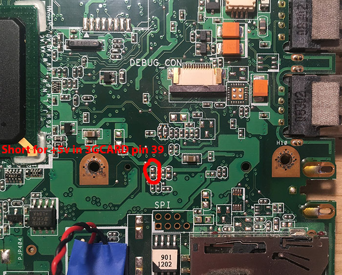
This could be handy if you are designing your own PCB to go into the slot or want to connect a regular USB device trough this slot.
MINICARD
TL;DR: A functional mini PCI-E connector, but without the USB lines.
I almost wrote this this is, for once, a standard-compliant mini PCI-E port, but
alas, the USB_D± pins are not connected, even though they should be by the
spec. But the rest of the interface is functional, including the PCI-E 1x line,
which is nice.
This slot is normally occupied by the WiFi adapter, which is kinda essential and therefore didn’t gain too much attention from the modder community. However, there are loads of interesting things one could try and plug into a spare mini PCI-E slot: high-performance network adapter, SATA controller or even external GPU 🤪 Might be worth the hassle of replacing the stock WiFi adapter with a USB one.
USB ports
TL;DR: there are at least 4 internal USB lines one could use, but all require some soldering.
USB ports are bread and butter for connecting extra bells and whistles to Eee PCs. Obviously, there are 3 external ports, which aren’t very convenient for internal mods. In addition there are a few more internal that could be repurposed for various needs.
I already mentioned above that IDE2 and 3GCARD have USB data lines on pins 36 and 38, which aren’t used by anything (at least in non-GO versions) and can be repurposed without a sacrifice. You’ll have to route 5v and GND from someplace else, though.
Next there’s BlueTooth adapter, which is probably the next-best trade for something cool. It uses a 10-pin connector, most of which are used for uninteresting stuff like toggling the radio on an off. For modding purposes the more interesting pins are:
- 1 —
GND. - 2 —
USB_D+. - 3 —
USB_D-. - 8 —
+3v.
The next option is webcam’s connector, which has all the standard USB leads:
GND, USB_D+, USB_D- and +5v. They seem the be using
SM04B-SRSS-TB(LFSN) PCB header for it, so potentially you could connect
through it without soldering on the motherboard. Also this is the only internal
USB port with 5v on it.
Technically, there’s also the SD card reader, which also has USB data lines, but they are routed in a really inaccessible way, so it’s better to leave it alone 😑
As a side note, it is possible to cram a USB hub board into Eee PC to get even more ports, and I read reports of people doing it with 701 models.
Internal audio
I wasn’t able to find reliable information, but MIC (internal microphone)
connector seems to be a digital protocol, probably
PDM. If you feel
adventurous, motherboard schematics is your friend.
Internal SPEAKERS, in opposite, are a straightforward analog stereo signal.
SPI
SPI is a well-known interface that is used for things like recovering from really bad BIOS update mishaps. The only relevant material for EEE PC 901 I found was a detailed posting by eeeuser.com member naviathan, who managed to re-flash BOIS using another linux machine. I really hope I won’t need it 😅
DEBUG_CON
Again, very little information about it but it appears to be a motherboard self-diagnostics port that uses ELPC or LPC protocol. The only somewhat “official” reference to it was ASUS LPC debug card, the rest was thousands of Chinese debug cards which claim to support it.
“Debug bus” always sounds interesting and hackable, but I couldn’t find any documentation about it whatsoever, so this will have to remain a mystery.
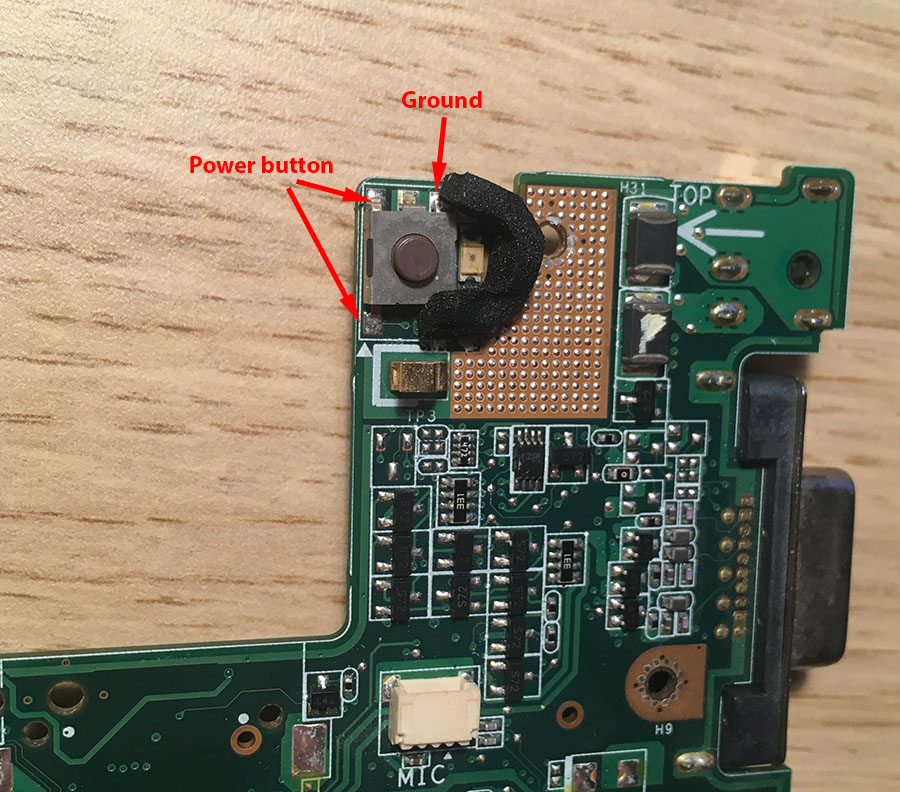
Power
Finally, one other thing that might be useful is the power button. The switch is located at the upper right of the top motherboard side, in case you want to turn it on while disassembled. And if you want to add a custom power button (warning, I haven’t tested that yet!) elsewhere, you need a momentary switch which would connect either of the “power button” contacts to “ground” as shown:
That’s all folks
I’ll try to keep the post updated with any useful info I gain, but that’s all I know so far. If you found mistakes or some new information, shoot me an email!
I hope you found it useful, cya 👋😃